
|
www.riscos.com Technical Support: |
To get the most out of your RISC OS computer, some knowledge of the hardware is important. This chapter introduces you to those features that are common to all RISC OS computers.
Each current RISC OS computer has a set of four chips in it, all designed by Acorn Computers Limited:
Together these chips are known as the ARM chip set.
Some machines combine the functionality of one or more of these chips as macrocells on a single chip: for example the A3010 and A3020.
The other main electronic components of a RISC OS computer are:
Exactly which components and devices are present will depend on the model of computer that you have; see the Guides supplied with your computer for further details.
The diagram below gives a schematic of an Archimedes 400 series computer, which may be viewed as typical of a RISC OS computer:
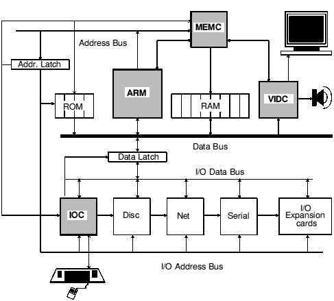
Architecture of an Archimedes 400 series computer
The ARM is a RISC (Reduced Instruction Set Computer) processor - it has a comparatively small set of instructions. This simplicity of design means that the instructions can be made to execute very quickly.
A traditional CISC (Complex Instruction Set Computer) processor, as used for the main processor of a computer, provides a much larger and more powerful range of instructions, but executes them more slowly.
A CISC processor typically spends most of the time executing a small and simple subset of the available instructions. The ARM's instruction set closely matches this most commonly used subset of instructions. Thus, for the majority of the time, the performance of the ARM is higher than that of comparable CISC chips; it is executing similar instructions more quickly.
The more complex instructions of a CISC chip are generally only occasionally used. For the ARM to perform the same task, several instructions may be necessary. Even then, the ARM still has a comparable performance, as it is replacing a single slow instruction by several fast instructions.
In summary, the simple RISC design of the ARM has these advantages:
Currently Acorn uses two different versions of the ARM processor. The newer ARM 3 is clocked at about three times the speed of the older ARM 2, and has a 4Kbyte on-chip cache. These two features mean that it delivers some three times the power of the ARM 2 (13.5 million instructions per second, or MIPS, compared to some 4 - 5 MIPS for the ARM 2).
From the programmer's point of view, there is little difference between the two processors. The ARM 3 supports the full instruction set of the ARM 2, and provides a few extra instructions: all but one of these instructions are used to control the ARM 3's cache.
The ARM uses 32 bit words. Each instruction fits in a single word. At any one time, the processor is dealing with three instructions:
The ARM has a 32 bit data bus, so that complete instructions can be fetched in a single step. Its address bus is 26 bits wide, so it can address up to 64 Mbytes of memory (16 Mwords).
The ARM has four different modes it can operate in:
The last three modes are privileged ones that allow extra control over the computer. They have been used extensively in writing RISC OS.
Note that if you force the ARM to change mode (usually done using a variant of the TEQP instruction) you must follow this with a no-op (usually done using MOV R0, R0). This is to avoid contention, giving the ARM time to finish writing to the registers for one mode before switching to the other mode.
The ARM contains twenty-seven 32 bit registers; you can access sixteen of these in each of the modes. Some of the registers are shared across different modes, whilst others are dedicated to one mode. In the diagram below, registers dedicated to a privileged mode have been shaded light grey:
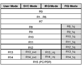
ARM registers
Only two of the registers have special functions:
One other set of registers is conventionally used by RISC OS for a special purpose:
All the remaining registers are general purpose.
R15 contains 24 bits of program counter and 8 bits of processor status register:
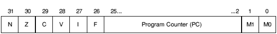
Bit usage in R15 by the PC and the PSR
| 0 | Enable |
| 1 | Disable |
| 0 | Enable |
| 1 | Disable |
| V | oVerflow flag |
| C | Carry flag |
| Z | Zero flag |
| N | Negative flag |
The program counter must always be word aligned, and so the lowest two bits of the address must always be zero. To maximise the available address space, these two bits are not stored in R15, but are appended to the program counter when fetching instructions, thus forming a 26-bit address.
R14 is used as the subroutine link register, and receives a copy of the return PC and PSR when a Branch and Link instruction is executed. It may be treated as a general purpose register at all other times. Similarly, R14_svc, R14_irq and R14_fiq are used to hold the return values of R15 when interrupts and exceptions arise, when Branch and Link instructions are executed within supervisor or interrupt routines, or when a SWI instruction is used.
R13 (and R13_svc, R13_irq) are conventionally used by RISC OS as private stack pointers for each of the processor modes.
If you write routines that are called from User mode and that run in SVC or IRQ mode, you will need to use some of the shared registers R0 to R12. You will therefore need to preserve the User mode contents on a stack before you alter the registers, and restore them before returning from your routine.
Note that the SVC and IRQ mode stacks must be full descending stacks, ending at a megabyte boundary. You are strongly advised not to change the system stack locations; if you do have to, you must be aware that they are reset to their default positions when errors are generated, and when applications are started.
FIQ routines need a faster response, so there are seven private registers in FIQ mode. In most cases these will be enough for you not to need to use any of the shared registers, and so you will be spared the overheads of saving them to a stack. If you do need to do so, you should for consistency use R13_fiq as the stack pointer.
You can use R13 and/or R13_fiq as conventional registers if you do not need to use them as stack pointers.
You will find details of the ARM's instruction set in Appendix A: ARM assembler.
The VIDC chip controls and provides the computer's video and sound outputs. The data to control these systems is read from RAM into buffers in the chip, processed, and converted to the necessary analogue signals to drive the display's CRT guns and the sound system's amplifier.
The VIDC chip can be programmed to provide a wide range of different display formats. RISC OS uses this to give you its different screen modes. Likewise, you can program the way the sound system works.
The VIDC chip has three buffers for its input data. These are used for:
Each of these buffers is a FIFO (first-in, first-out). The VIDC chip requests data from RAM as it is required, using blocks of four 32-bit words at a time. The MEMC chip controls the addressing and fetching of the data under direct memory access (DMA) control.
Data from the video buffer is serialised by the VIDC chip into 1, 2, 4 or 8 bits per pixel. The data then passes through a colour look-up palette. The output from the palette is passed on to three 4-bit digital to analogue converters (DACs), which provide the analogue signals needed to drive the red, green and blue cathode ray tube (CRT) guns in the display monitor.
The palette has 16 registers, each of which is 13 bits wide. This supports a choice from 4096 different colours or an external video source.
The registers that control the video system give a wide choice of display formats:
If needed, support is provided for:
The cursor data controls a pointer that is up to 32 pixels wide, and any number of rasters high (although RISC OS restricts the cursor to a maximum of 32 rasters in height). Its pixels can be transparent (so the cursor can be any shape you desire), or can use any three of the 4096 possible colours.
The cursor may be positioned anywhere on the screen within the border.
The sound data consists of digital samples of sound. The VIDC chip can support up to eight separate channels of sound. It provides eight stereo image registers, so the stereo position of each channel can be independently set.
The VIDC chip reads data from the buffer at a programmable rate. The data is passed to an eight bit DAC, which uses the stereo image registers to convert the digital sample to a stereo analogue signal. This is then output to the computer's internal amplifier.
The IOC chip provides the facilities to manage interrupts and peripherals within your RISC OS computer. It controls an 8 to 32 bit Input/Output (I/O) data bus to which on-board peripherals and any I/O expansions are connected. It also provides a set of internal functions that are accessed without any wait states, and a flexible control port.
The following internal functions are provided by the IOC chip:
The IOC is connected to the rest of the ARM chip set by the system bus. It provides all the buffer control required to interface this high speed bus to the slower I/O or expansion bus. The IOC supports:
Both the IOC and peripherals are viewed as memory-mapped devices. Most peripherals are a byte wide, and word aligned. A single memory instruction (LDRB to read, or STRB to write) can be used to:
The IOC can support a wide range of peripheral controllers, including slower, low-cost peripheral controllers that require an interruptible I/O cycle.
The MEMC chip interfaces the rest of the ARM chip set to each other and to the computer's memory. It uses a single clock input to provide all the timing signals needed by the chip set.
MEMC provides the control signals needed by the memory:
Up to 32 standard DRAMs can be driven, giving 4 Mbytes of real memory using 1 Mbit devices.
Fast page mode DRAM accesses are used to maximise memory bandwidth, so that slow memory does not slow the system down too much.
MEMC maps the physical memory into a 16 Mbyte slot, the base of which is at 32 Mbytes. RISC OS does not address this slot directly, though; instead it addresses another 32 Mbyte logical slot within the 64 Mbytes logical address space supported by the ARM's 26-bit address bus. Each page of the slot that RISC OS addresses can be:
RISC OS can only read and write from pages that have a one-to-one mapping. One-to-many mapping is used to 'hide' pages of applications away when several applications are sharing the same address (&8000 upwards) under the Desktop. These pages are, of course, not held at &8000.
The computer's physical memory is divided into physical pages. Likewise, the 32Mbytes of logical space is divided into logical pages of the same size. MEMC keeps track of which logical page corresponds to which physical page, mapping the 26 bit logical addresses from the ARM's address bus to physical addresses within the much smaller size of RAM.
MEMC has 128 pages to use for its memory mapping. Each page has its own descriptor entry held in content-addressable memory (or CAM). This simple structure allows the translation (of logical address to physical address) to be performed quickly enough that it does not increase memory access time.
In general, all 128 pages are used to map the RAM. Note that this is not always the case; for example, the Archimedes 305 uses only 64 pages.
If MEMC does use all 128 pages (or any other constant number), then:
MEMC addresses a maximum of 4 Mbytes of memory. Machines with more than 4 Mbytes fitted have an extra MEMC chip slaved to the master MEMC chip for each additional 4 Mbyte fitted, so the page sizes are the same as for a 4 Mbyte machine.
The table below shows this. The values are those used in Archimedes computers, and may be viewed as typical of RISC OS computers. They should not be relied on for programming though; future RISC OS computers may not use 128 pages per MEMC chip, leading to anomalies such as those in the first row (the Archimedes 305):
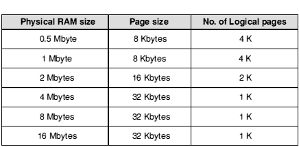
Page sizes for Archimedes computers
If you need to find out a machine's page size and so on, use OS_ReadMemMapInfo.
RISC OS programs a minimum of 128 pages, even if it actually uses fewer pages. This is so that:
MEMC can run in three different protection modes: Supervisor, Operating System, and User. Each page of memory has one of three different protection levels: 0, 1 and 2. (There is also a level 3, which is identical to level 2.) Whether you have read and/or write access to a page of memory is determined by MEMC's current protection mode, and by the protection level of that page:
RISC OS itself does not use Operating System mode.
If an attempt is made to access protected memory from an insufficiently privileged mode, MEMC traps the exception and sends an abort signal to the ARM.
The resulting memory map is shown below. You can only access the areas shaded grey if you are in one of the ARM's privileged modes (SVC, IRQ or FIQ), which force MEMC to Supervisor mode by holding a pin high:
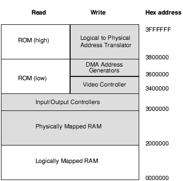
Memory map of a typical RISC OS computer
MEMC also provides three programmable address generators to support direct memory access (DMA). They support:
If you need to find out more about ARM assembler and the ARM chip set, there are a number of sources you can turn to:
In addition, a number of other publishers have produced books covering these topics - such is the interest in the ARM chip set.